Signal Integrity Design Considerations
The second technical deep-dive into an electronics topic that probably isn't particularly relevant to the hobbyist-level

Intro
So here goes another post about a tangential electronics topic so that I don't feel so bad about not making progress any actual projects. I can only hope that maybe one person gets a slither of enjoyment from this.
So, what topics am I going to cover?
- GND return paths (layers, vias, etc.)
- PCB stackups
- Length matching
Well those are the headings, but the GND return path section makes the other two look like throwaway comments and to be honest that's the one thing that I want you to go away from this with (if you are ever likely to make a PCB) - GND returns are critical for signal integrity and should be treated as such.
GND Return Paths
Proper ground return paths are critical for preventing signal integrity problems. This is important both with radiated immunity and radiated emissions (as well as many other EMC tests), but even for hobby projects where EMC regulations aren't a concern it will give you better odds of a working design (particularly as you reach higher and higher speeds).
Robert Feranec has a lot of good videos about this (particularly ones featuring Eric Bogatin), although they can be quite drawn out sometimes (usually ~1hr long).
Low Frequency vs High Frequency
All return currents will follow the path of least impedance, but what the determining factor of the impedance is depends heavily on the frequency content of the return current (and therefore the signal/power it originated from)
Currents flowing at low frequencies (<100 kHz) will follow the path of least resistance - this is most often the physically shortest path that's available to it.
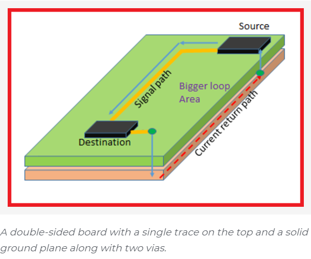
At higher frequencies (>10 MHz) return currents will tend to follow paths that mirror the route that the signal/power takes in the other direction. Much like the decoupling capacitor discussions from my previous post, this is caused by the parasitic inductance which is created by large loop areas.
Note: A digital signal will have much higher frequency harmonics (and therefore higher frequency components of current flow) than the nominal frequency - far more signals than you might expect will at least have some high frequency components in digital circuits.
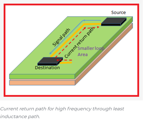
The return path on a ground plane mirroring the signal path directly below the signal/power trace has the smallest possible loop area, and is therefore the path of lowest inductance. As such the majority of the high frequency current will follow this path (where possible) rather than the "shorter" path with the lower resistance.
Images showing the path return currents will tend to take for a low-frequency signal on the left and a high-frequency signal on the right
Note that at high frequency (>30 MHz for 1-oz copper, >120 MHz for 1/2-oz copper), the return currents will also more readily flow on the nearest edge of a plane or via to that of the signal it is paired with due to the skin effect. As such, at high frequency, each GND plane effectively acts as two separate GND planes. See Section 10.6.1 & 16.3 of Henry Ott's "Electromagnetic Compatibility Engineering" for more detail on this.
For high frequency signals then, it is relatively easy to keep the return currents separate between the various signals. This is why having a solid ground reference (and therefore return path) for every high-speed signal is so important for EMC & signal integrity - simply route everything with solid adjacent ground planes and the return currents will basically sort themselves out as long as you follow the guidelines in the section below.
GND Return Paths For Power Traces/Planes
Do not neglect the ground return path of power traces/planes. While they are (in theory) low frequency DC, there will be very high frequency components of voltage/current on the otherwise DC rail caused by the high-speed components that are drawing power from it.
If you are using a power plane (a full layer dedicated to power), it should have a GND plane directly vertically adjacent to it. Ideally, these should also be closely coupled (as small a distance as possible) to take advantage of the intrinsic inter-place capacitance, as well as minimising the loop area for return current going through vias (many of the tips in my capacitor post assume this is the case).
If there is not space for an adjacent GND plane (and possibly also if they otherwise wouldn't be closely coupled), then it is preferable to route the power as traces on a signal layer which is tightly coupled GND plane.
Do not fall into the trap of thinking that using a power plane instead of traces will inherently lower the power supply inductance (and therefore reduce noise) - if the GND return path for the high frequency current flow of the supply is not considered (and the loop area minimised) then this will often make things worse than routing on a thinner trace (with a well-coupled GND return) could have achieved.
GND Transfer Vias
GND transfer vias are required when the reference plane of a signal changes. This allows the return (GND) current to change between the various GND layers within a multilayer board.
A properly via-stitched board will go some way towards this (particularly for low to mid frequency signals), but a significant diversion to the nearest via for some signals can introduce enough of a discontinuity that there will be signal integrity problems if a dedicated transfer via is not present. Anything particularly high frequency should therefore have dedicated GND transfer/return vias present in close proximity.
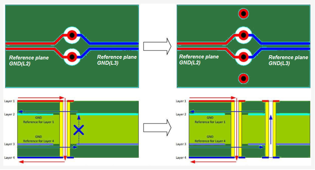
Note: a signal can transfer layer without changing reference plane (for example a signal changing from layer 1 to 3, with a GND plane on layer 2) which would not necessitate a GND return via. As such, a tightly coupled set of signal-GND-signal layers is great for routing of high-speed signals (although generic PCB stackups tend to leave layers in pairs with large gaps between). The skin effect mentioned above in the LF/HF Section would normally prevent the return current from changing "side" of the return plane, however the via for the signal changing layer provides an edge in the plane for the return current to transfer, so you don't need to worry about it. Neat!
Additionally, if power planes are used as reference planes then stitching capacitors (and vias) can be used to transfer the reference plane from a ground to a power plane for high frequency return currents, however this is not recommended as the next designer (or yourself in the future - sometimes even more problematic...) needs to be very aware of this before they start making changes - for things which are not low-cost & high volume products, adding additional ground layers is far more preferable).
Traditionally, hobby projects are the sort of application where trading away good signal integrity for fewer layers and a cheaper board would make sense, however 4, 6, or even 8-layer boards are now so cheap (all hail JLC PCB, #not-sponsored) that it often does make sense to go for them - sometimes at no additional cost!
Split Reference Planes
Splits in the reference plane of a signal below the trace where the return current should flow are to be avoided at all cost. The increased path length of the return current as it goes around the split in the reference plane (shown in below in "a.") causes a significant discontinuity and can lead to degradation of the signal integrity (and radiated emissions).
As far as split planes go, assume all signals are high frequency and require a solid return path directly below them.
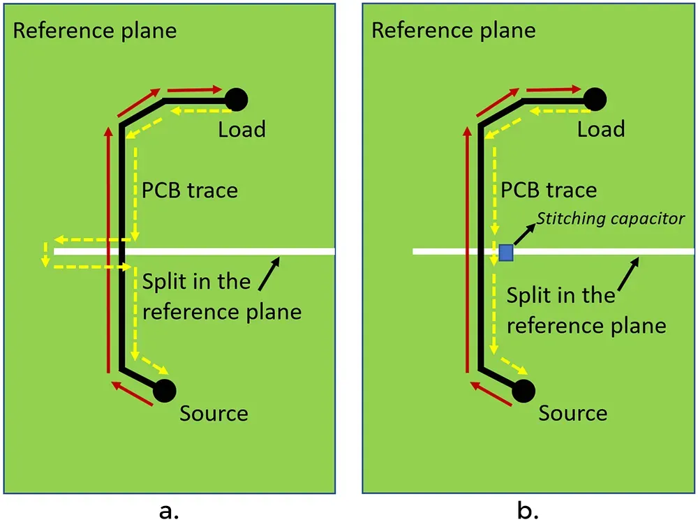
If you must route a trace over a split in a plane and you must have a split in the plane below, then a stitching capacitor can be used to allow the high frequency currents flow "across" the split without connecting the planes at DC.
This is still not ideal though, as vias are required to transfer the reference plane to the top or bottom layer and back again which will still cause a significant discontinuity. It also requires the next engineer to know/understand what has been done which will likely not be immediately obvious to most - it would be very easy to move the trace along the split without moving the stitching capacitor with it.
The only legitimate reason you should really have a split plane for is isolation, at which point you shouldn't be running traces across anyway. Get rid of them.
GND Planes - To Split, or Not To Split
A continuation of the topic above, but something I think some people might not grasp from just that section - like many of the issues I covered about capacitors, years ago it was common-practice/state-of-the-art to split reference/return planes in order to prevent the return currents of high-speed digital signals from interfering with low-speed sensitive/analogue signals.
This should be ignored - even with poor implementation, splitting ground planes will usually cause more problems than it solves (particularly in most designs I've worked on where high-speed digital signals are common and absolute precision of analogue circuitry is not paramount). Proper partitioning/placement & routing of the PCB to reduce crosstalk/interference is always a better solution.
From Henry Ott Consultants - Grounding of Mixed Signal PCBs:
High frequency digital ground return currents want to return directly underneath the signal trace. This is the lowest impedance (lowest inductance) path. The digital ground currents have no desire to flow through the analog portion of the ground plane and corrupt your analog signal. Why then do we need to split the ground to prevent the digital current from doing something that it does not want to do anyhow? Therefore, I prefer the approach of using only one ground plane and partitioning the PCB into digital and analog routing sections. Analog signals can then be routed only in the analog section of the board (on any layer), and digital signals can be routed only in the digital section of the board (on any layer). What causes problems is when a digital signal is routed in the analog section of the board, or visa versa.
A PCB with a single ground plane, partitioned into analog and digital sections, and discipline in routing the signals can usually solve an otherwise difficult layout problem, without creating the additional problems caused by a split ground plane. If the layout is done properly, the digital ground currents will remain in the digital section of the board and will not interfere with the analog signals. The routing, however, must be checked carefully to assure that the above mentioned routing restrictions are adhered to one hundred percent! The key to a successful mixed signal PCB layout, therefore, is proper partitioning and routing discipline, not a split ground plane.
Many A/D converter manufacturers, while suggesting the use of split ground planes, state the following in their data sheets or application notes: "The AGND and DGND pins must be connected together externally to the same low impedance ground plane with minimum lead length. Any extra external impedance in the DGND connection will couple more digital noise into the analog circuit through the stray capacitance internal to the IC." Their recommendation is to connect both the AGND and the DGND pins of the A/D converter to the analog ground plane. This approach has the potential of creating a number of additional problems. Can you list some of these problems? What do you connect the ground side of the digital power decoupling capacitor to? The analog plane or the digital plane?
A much better way to satisfy the requirement of connecting AGND and DGND pins together through a low impedance, and not create additional problems in the process, is to use only one ground plane to begin with.
The key to determining the optimum board layout is to think, how and where do the return currents flow?
If you are still skeptical about using a single ground plane on your mixed signal boards I suggest you do the following experiment. Layout the board with a split ground plane, but provide means for connecting the two planes together every 1/2 inch with jumpers or zero ohm resistors. Route the board properly, with no digital traces (on any layer) over the analog plane and no analog traces (on any layer) over the digital plane. Build the board and test it's functionality and EMC performance. Connect the planes together and test the board again for functionality and EMC performance. I think that you will find that in almost all cases, both the functional performance and the EMC performance of the board will be better with the single ground plane. If you do the experiment send me an e-mail letting me know of your results.
It is almost always better to have only a single reference plane for a system!
Summary:
- Partition your PCB with separate analog and digital sections.
- Do not split the ground plane. Use one solid ground plane under both analog and digital sections of the board.
- Route digital signals only in the digital section of the board. This applies to all layers.
- Route analog signals only in the analog section of the board. This applies to all layers.
- The key to a successful PCB layout is the use of routing discipline.
From learnemc - Some of the Worst EMC Design Guidelines:
Solid ground planes should be gapped between analog and digital circuits.
This is probably a close second in the competition for the worst EMC design guideline ever conceived. There are some (very few) situations where gapping a ground plane between analog and digital circuits is a good idea. These situations are always related to a need to keep low-frequency (< 100 kHz) currents produced by a noisy circuit from sharing the same copper return path as currents in a circuit that is sensitive to currents approximately 3 orders of magnitude lower. Unfortunately, gapping a solid ground plane can cause enormous problems by interfering with the flow of high-frequency currents and generating voltages that ultimately result in radiated emission problems. In many cases, leaving the plane solid and letting both circuits share the plane is fine. In situations where low-frequency isolation is required, it is almost always better to provide separate return paths for these circuits. This is generally accomplished using a trace or plane on a different board layer.
The ground plane under the I/O (connectors) should be separated from the digital ground plane with one connection point between them.
This guideline was not unreasonable 30 years ago when most boards had two layers, were less densely populated, and operated at relatively slow speeds. However, today this is generally one of the worst-possible ways to layout a ground plane. Generally, the goal should be to achieve a low-impedance connection between chassis and digital ground at radiated emissions frequencies (e.g. above 30 MHz) and control the flow of any low-frequency (e.g. <100 kHz) currents by isolating the chassis from the digital ground at low frequencies. This layout accomplishes the opposite of that. As a result, products employing this design usually have lots of capacitors bridging the gap between the digital and chassis grounds. This effectively forms a notch filter of questionable value.
Low-frequency isolation and high-frequency bonding are much better achieved by putting the chassis ground on a separate layer and overlapping it with the digital ground. This allows a good high-frequency connection to be made between them using multiple low-inductance SMT capacitor connections. A low-frequency connection can be made between digital ground and chassis ground at the single-point where it makes the most sense; which may or may not be in the vicinity of the I/O.
The general rule-of-thumb that a solid ground plane should never be split applies here. If the ground plane needs to be cleared out of a particular area, (e.g. under magnetics, power inverters, or for high-voltage isolation) that is often fine. Splitting/gapping a ground plane, however, is almost always a bad idea.
Single-point grounds should be used for low-frequency circuits. Multi-point grounds should be used for high-frequency circuits.
While the underlying sentiment of this guideline is not necessarily incorrect, system designers that do not understand the difference between "ground" and "current return" use this guideline to justify some terrible designs. At low frequencies, we do not want all return currents to flow through a single point. Yet that is precisely what happens when people blindly try to apply this concept. Generally speaking, we want to control the flow of low-frequency currents by limiting the options. We control the flow of high-frequency currents by providing one good option. The concept of single-point and multi-point grounds is rarely helpful and often a significant source of bad design ideas.
From Advanced PCB Design and Layout for EMC Part 4 - Reference planes for 0V and power:
Never split a 0V plane just because ‘we always used to do it’, or because any EMC guideline or IC application note says so. It used to be traditional to split planes between analogue and digital areas, but the author has found on hundreds of PCB designs since 1981 that PCBs can generally be designed to have better signal quality and EMC by using one 0V plane for all the circuits. Many other electronic designers have found the same. It is not unusual for analogue signal quality to be significantly better than what had previously been considered for decades to be the state of the art.
Due to the small silicon processes used in modern ICs, split 0V planes should now only be used as part of a well thought-out EMC plan, implemented by people who are sufficiently EMC-competent and equipped with all necessary EMC tools. 0V plane splits of any practical width don’t work well as splits above 1GHz anyway, and hardly have any effect >2.5GHz, due to the reducing impedance of the stray capacitance across the split as frequencies increase.
The problem is that – for traces that must cross a 0V plane split – it is very important indeed to maintain the intimate proximity of the send and return currents. This is not always easy, or low-cost, but if it is not done correctly the resulting degradation in EMC will be much worse than the benefits that could ever be hoped to be achieved by the use of a split. How to deal with traces that cross plane splits is discussed in the next section.
One way of dealing with uncertainty over whether to split a 0V plane or not, is to construct a prototype PCB designed to provide both options, then test it to see what works best.
Because the circuit has been laid out on the PCB in segregated circuit zones, as described in [7], it is easy to split the 0V plane between these zones. Then pad patterns that can be used for small capacitors, resistors or zero-ohm links should be placed at regular intervals around all the perimeters of all of the plane splits, so that they can be used to connect between the planes on either side of the split. These are often called ‘plane stitching’ components, and Figure 4M shows the general idea.
Never allow a trace to cross a plane split because it is difficult to control the trace’s return RF currents (which flow in the surface of the adjacent plane or planes) so as not to cause EMC problems. Some designers think that low-frequency analogue signals or power have no RF content so there is no need to worry about the RF return currents for such traces, but such signals and power are always vulnerable to RF interference, so the same PCB EMC design techniques should be applied.
In general, most hobbyists (and perhaps even most companies) are not "sufficiently EMC-competent and equipped with all necessary EMC tools" that we can make good use of GND plane splits for EMC (they are however required in some places for functional safety isolation barriers).
As such, use a single GND for AGND, DGND, SGND, PGND, etc. In my, albeit limited, experience I have not (yet) encountered significant problems with noise due to this and have witnessed significantly reduced radiated emissions by following this practice.
Cuts in the GND planes should only be deliberately made if you are absolutely sure about what you are doing (and ideally have had thorough review & confirmation from other competent/senior engineers).
Care should be taken to place & route the design such that the low-frequency sensitive analogue return currents that flow through the lowest resistive path naturally do not conflict the high-frequency return currents of digital electronics which follow the lowest inductance path, rather than forcing this divide by splitting GND planes.
Why do device packages still have split rails exposed on pins?
If split grounds are so bad, then why to device manufacturers allow you to do it by providing separate pins like VSSA? Besides following out-of-date design practices, either because they are believed to still be correct or "it worked before so why change it?", there is some merit to having separate GNDs internal to an IC with separate external connections.
Citation needed (and not provided), but this is my best justification to why they do (and should) still exist:
-
They allow for power to be completely disconnected (including GND) from individual parts of the IC. This can be useful for testing, particularly for the IC manufacturer.
-
Within the IC it can prevent return currents from mixing which would otherwise degrade the signal integrity of the device. This is particularly important where the IC may not have an internal GND plane and instead route return currents through "traces".
- This also applies to the interconnect from the device die to the PCB GND plane through the via, pin, bond wire, etc. As such it is slightly less important on device packages with a thermal pad that allows the device to better bond to the PCB GND plane over a large area at a lower inductance.
-
The GND pins can be placed on opposite sides of the package to better isolate return currents from each other (by allowing placement & routing to be performed such that low-resistance LF & low-inductance HF return paths do not intersect without requiring split ground planes)
GND plane voids
It can be easy to fall into the trap of thinking that, with an unbroken GND plane adjacent to your signal layer, there are no restrictions with where you can route traces - there are no split planes, so nowhere to avoid, right? Not quite.
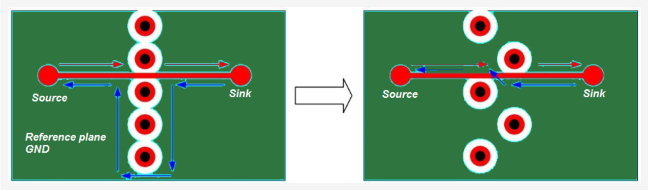
The image below shows an example of a via fence that is spaced enough that a signal is able to pass through, but close enough that the ground plane pour is not cut off causing the same effect as a split plane. Even if it doesn't cut off the ground plane completely, bad via placement can also cause high current densities, once again leading to a discontinuity in the reference plane (leading to bad signal integrity).
The example above might perhaps feel a little contrived (and perhaps only possible with some non-ideal design rules), but by no means impossible.
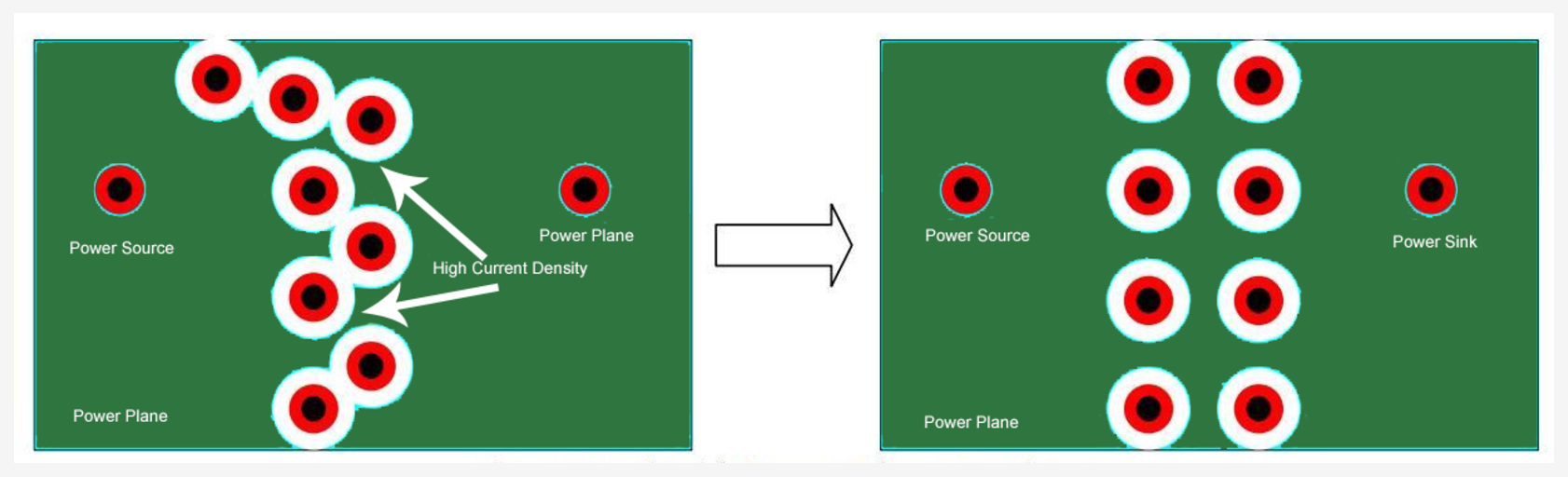
Below, however, is a much more common example of how this can accidentally be done when breaking out a device (particularly QFN/QFP packages with tight pitches).
The images show a "before", where bad placement of vias has put a split in the reference plane, and "after", where this has been fixed by properly spacing them out and allowing GND return paths to flow between the vias much closer to the signal traces.
A good example of how splits in the GND plane can be accidentally made (where traces are also being run directly over the split). The image on the right shows how careful staggering of the via placement
Power & signal plane stackup
Finally, no more GND return chat.
Surprise - layer stackup design is all about GND returns! Alright, there's a bit more to it...
There are four main factors/considerations that are important important to consider when choosing a stackup. They are, in no particular order:
- The number of layers
- The number (and types) of planes
- The ordering/sequencing of layers
- The spacing between layers
In a multilayer stackup, the following objectives should be targeted:
- Each signal layer should be directly adjacent to a plane (ideally ground)
- Each signal layer should be tightly coupled to their adjacent plane
- Power planes should be tightly coupled to an adjacent ground plane (if not then it is preferable to remove the plane and route them on a signal layer instead)
- Multiple ground planes are preferable
- When critical signals are routed on more than one layer, they should be confined to just two layers on either side of the same ground plane (as discussed below in the Section on routing)
It is often difficult to meet all of these without some compromise (either on one of these points, or on cost of the PCB due to adding additional layers)
Note: If you happen to use Altium, use "signal" layers/planes for everything (even power planes), Altium inverts the power plane layers so that it indicates etched copper rather than filled which can be very confusing/annoying to deal with.
Routing high speed clocks & other critical high-speed signals
In order of preference (per Henry Ott's "Electromagnetic Compatibility Engineering", Section 16.3.4) high-speed/critical signals should be routed:
- On only one layer, adjacent to a reference plane
- On two layers that are adjacent to the same reference plane
- On two layers adjacent to two separate reference planes (with the same net), with transfer vias added
- On two layers adjacent to two separate reference planes (different nets) with transfer vias and stitching capacitors added
- On more than two layers
Suggested Stackups For Good Signal Integrity
I don't want to claim that any of these are perfect, but they're a pretty good place to start and give some reasonable examples of what you should be looking for with good stackup.
Signal layers in the examples below can be swapped for full power planes (if not many signal routing layers are required) or used to route power traces alongside signals (where fewer dedicated power planes are available than are required).
4-Layer
| 2-2 1 Signal, 1 Signal/Power |
|---|
| ----- Signal ----- GND --- ----- GND ----- Signal/Power |
6-Layer
| 2-2-2 2 Signal, 1 Signal/Power |
3-3 2 Signal, 2 Signal/Power |
|---|---|
| ----- Signal ----- GND --- ----- Signal/Power ----- GND --- ----- GND ----- Signal |
----- Signal ----- GND ----- Singal/Power --- ----- Signal/Power ----- GND ----- Signal |
8-Layer
| 2-2-2-2 2 Signal, 2 Signal/Power |
3-2-3 2 Signal, 3 Signal/Power |
|---|---|
| ----- Signal ----- GND --- ----- Signal/Power ----- GND --- ----- GND ----- Signal/Power --- ----- GND ----- Signal |
----- Signal ----- GND ----- Signal/Power --- ----- GND ----- Power --- ----- Signal/Power ----- GND ----- Signal |
Length Matching
Some signals are required to be length matched to each other in order to prevent issues. This happens when signals must be synchronised (e.g. data to a clock signal), where propagation delays could cause it to clock the wrong bit, an edge, or violate setup/hold times.
This will all depend on the frequency things are running at, and the distance they are mismatched by, and therefore whether the amount of time they will be off by is close to or greater than the time between each sample/bit.
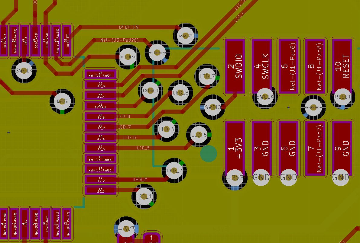
For Ethernet PHYs, this TI layout checklist gives some pretty strict targets to aim for (as well as a bunch of other guidance like GND transfer vias, keepouts, & spacing guidelines).
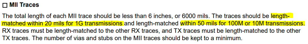
In practice for MII you can mostly get away without length matching (as long as it's across short enough distances) and for RMII you probably only need it if things are a little bad distance/matching wise.
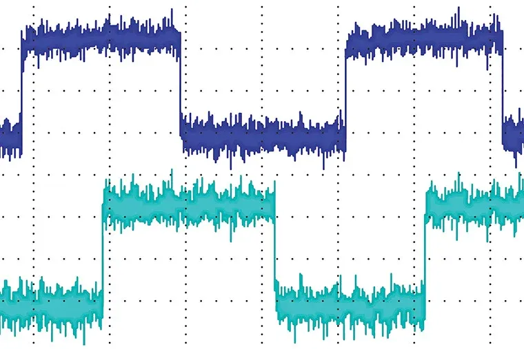
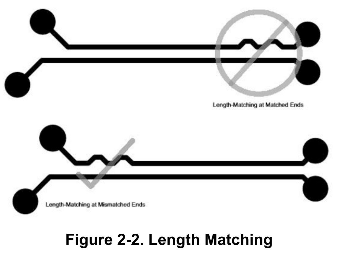
Additionally, for differential signals intra-pair length matching should be performed near to where where the length mismatch originates so that the location of the deviations are matched as well.
This prevents one side of the balanced/differential signal from getting too far out of phase with their counterpart as they propagate down the wires:
This isn't as important for single-ended/unbalanced signals which use ground for their return path (which at high frequency should have a lovely unbroken ground plane underneath allowing the return current to self-length-match to it's heart's desire) - it's pretty much just the arrival time that matters.
That's your lot
Well done - you've made it to the end of this yawn-fest! Even more so if you even read the whole lot rather than just scrolling to the bottom.
Hopefully you've learned something useful, or if not, that I haven't bored you to the point of unsubscribing.
This will probably be the last deep-dive into pretty technical electronics topics for a while though, so at least there's a small silver lining!