The Arduous Process of Hardware-Software Integration

I've realised I'm going to need to split this into quite a few posts if I want to have anything resembling frequent updates, rather than one mega-post in like 6 months. So here's, what I presume will be, the first of a series of posts talking about the software (and FPGA?) development for the modular motor controller PCB I've designed.
The Rough Plan
There's a lot of features that need testing on the STM32, and once a proof of concept is working there will be plenty more to add on top to make a fully featured system. As it stands, here's what the breakdown of that work is in my mind:
- Something (blinky?) running
- Debug UART writing
- Implement debug message/command interface
- ADC supply voltage sensing
- ADC motor current sensing
- I2C EEPROM reading & writing
- DAC motor current limit setting
- FPGA SPI interface
- FPGA position sensor reading
- FPGA PWM outputs
- Basic Motor control
- CAN bus read & write
I'm sure I'll think of more that needs doing while I work my way through that list - and remember this is just to test the hardware. There's plenty more software development to do before it's competition ready, particularly if I want to achieve some of my stretch goals such as software updates over CAN, or automatic calibration & PID tuning.
As long as the hardware is good the software can follow, or at least that's the theory. So let's get to testing it then, shall we?
How Far Have I Got?
Well I've ticked off all the easy ones so far. But you have to start somwehere, and it's still a decent amount of progress with plenty to talk about. A brief disclaimer though - a lot of this is probably going to be a little dry, the most exciting this gets is a few screenshots of some debug print statements. If you're still here though, then let's delve into some of the details of the software testing that I've done so far.
Blinky
Naively, you might think that just getting a simple LED to flash by toggling a digital output would be the easiest thing on the list. Getting anything to run on a new design though can sometimes be quite a large hurdle.
Last time around for example, in the run up to PiWars 2024, I had a pretty difficult time with setting the option bit in the STM32 to use another option bit for the BOOT0 function rather than the hardware pin. As per usual, the root issue were my lackluster reading & comprehension skills causing me to set the bits the wrong way round which kept putting the STM into DFU (Device Firmware Update) mode.
This time around at least I more or less knew what I was doing, given the design for the STM was largely the same. After a bit of clock management to get it to run using the internal oscillator and flashing an image onto the STM - bingo! One blinky, in all its pixelated glory:
UART Debug Command Interface
Unfortunately I don't have any good pictures of the base interface though, because I went straight onto the next step trying to get the ADCs working. There's a decent example of it in action further down though.
Essentially what I've made is a relatively generic/extensible framework for adding debug commands to the UART interface of the STM which can take several arguments and run whatever functions I desire. This then allows me to run experimental code, change settings, or really anything else I desire, just by sending commands over the debug UART. I've found it significantly improves the rate I can develop and test new code compared to throwing together a new program in the main loop when I want to trial something new.
It's not exactly very efficient, but it doesn't need to be since it's just for development. Alright, so we ran everything over this interface last time, but it'll be different this time...
The formatting could maybe do with some improvement (see the janky text alignment below), but it's functional. I'd aslo like to expose the same interface over the CAN bus without having do duplicate the functions, but that's an integration problem for later on.
Reading ADCs
Analogue to digital converters, one of the more basic microcontroller peripherals, and one of the ones that I've historically had an uncharacteristically large number of issues with.
And this time was no different, it took me unreasonably long to get them running in a simple blocking operation. But after plenty of issues, most notably with them being configured with differential inputs rather than single-ended, I finally managed to get them working.
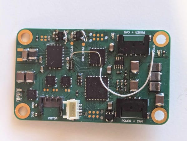
Once they were working though, this immediately indicated another issue - I'd designed the "VSUPPLY" (bus/input supply rail) sense voltage divider upside down putting 10-20V onto the ADC pin. Oops. Luckily, after swapping the resistors around, the ADC seemed to be undamaged and it read the voltage correctly.
The image below shows the basic commands from the debug interface from before (help, id, and LED control), as well as the newly added supply voltage and current sense analogue read functions in action.
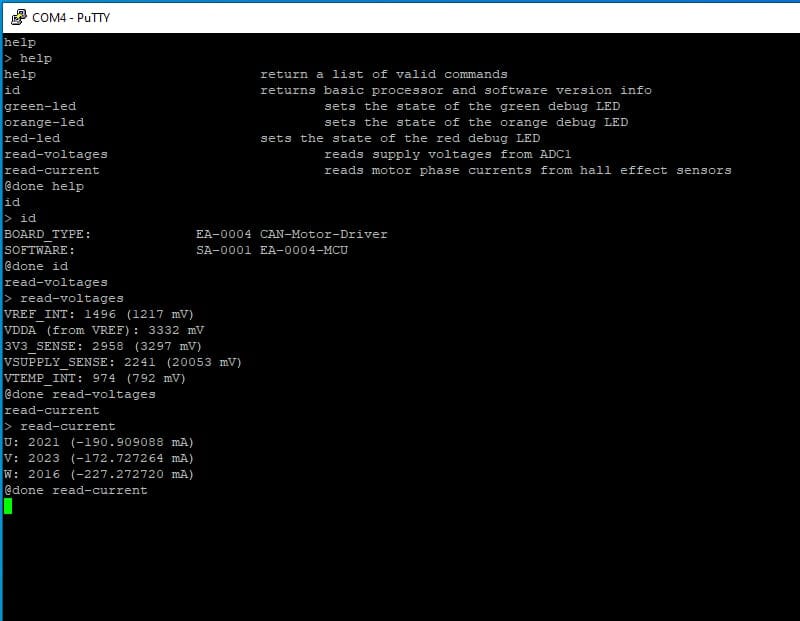
The supply voltage results are pretty reasonable, and while adjusting the input supply the result still matched pretty accurately, so I'll call that a success.
The current-sense values are noticeably off though, all reading around -200mA. I don't have a motor (or anything else) connected at the moment, so there shouldn't be any current flowing. There's clearly an offset error here then, but that's a problem for later though when I get to writing some calibration functionality. For now, I know that the ADCs and their inputs are vaguley working. Maybe when I get some basic motor commutation working I can also check that the readings increase when current is flowing.
For now though, it's time move on to the next hardware test.
I2C Configuration EEPROM
I think I probably said before, this isn't strictly required - I could use some of the STM32 flash for storing things like configuration & settings, but I like the idea of having a segregated EEPROM so that I can blindly reflash the STM without worrying about wiping the settings. It's also pretty tiny - at least when you use the correct package...
This was a super easy chip to integrate with though, it only took me an hour or two to read the datasheet and write some code. After adding some commands to read and write, and fixing the inevitable build errors, my code even worked first time which almost never happens! So, like I said, super easy.
Below you can see a read, write, read of the same address showing that the value updates.
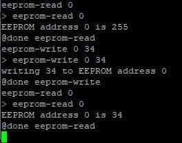
So there you go, 2kb of memory (256 bytes) to use for settings. Exactly what those will end up being is, like a lot of things right now, a problem for future me.
DAC Control
I was initially worried that getting this working would be as complicated and difficult as the ADCs had been, but it wasn't to be. I think it only took about an hour to throw something together and after once again fixing the inevitable compilation errors, it also worked first time!
The DAC output is used for setting the hardware current limit of the DRV8316 motor driver, which I cant test just yet since I don't have a software interface to the FPGA which controls the drive enable & PWM signals.
Measuring the output pin with a multimeter is enough confirmation for now while I work on implementing some of the FPGA functionality.
But a Drop in the Ocean
That's enough for this post I think. I've only scratched the surface of the work that needs to be done with the hardware testing and software integration for this PCB, and I've accrued several hardware mods on my way here which I'll talk about another time (once the Rev-B motor driver update is complete), but it feels good to be making steady progress with the software development - even if it isn't at a breakneck speed.
