Motor Driver FPGA Development

Perhaps you're wondering:
- What is an FPGA?
- Why would you use an FPGA?
- How do you use an FPGA?
Or maybe not, I don't know what you're thinking. Either way, I'll try to answer these questions since FPGAs are relatively niche in the world of hobby electronics and I really like them. If you happen to already be familiar with FPGAs, please try to forgive me for all the interesting details that I'm about to completely gloss over.
What is an FPGA?
There are plenty of sources that will probably explain this a lot better than I will, here goes nothing.
The short answer is that it's a "Field Programmable Gate Array", but on its own that isn't particularly helpful. A slightly better short answer is that they are integrated circuits which contain a matrix of programmable logic gates.
To better explain, perhaps a hypothetical might help:
Imagine you want a chip that can perform any logic function (AND, OR, NAND, NOR, XOR, etc). You could put all of those functions onto an IC and then have a MUX (multiplexer - essentially a programmable switch) determine which one is connected to the I/O pins. This would, however, require an unreasonable amount of pins if you wanted to do anything remotely complex.
So, to make an arbitrary logic function, you might instead use an EEPROM (programmable memory). By programming the contents of the memory, the address lines can be used as the logic function input, and it will output whatever arbitrary value has been programmed for the set of given inputs. Used in this context an EEPROM is more commonly know as a look-up-table or LUT. Ben Eater has a great video on this subject.
To take this a few steps further, you could put many of these on to a single chip with D-type flip-flops (registers) and their outputs so that they can be used to make synchronous circuits rather than just combinational ones - you might call each of these a logic block or element - see the picture below for an example of this, although the specific implementation of a "block" varies greatly between different FPGAs.
Then you could join everything with programmable interconnects and drive all of the programmable/configurable elements of this design with a massive shift registers which loads from a configuration memory when it powers on.
After all this, you'd get something that looks a little like:
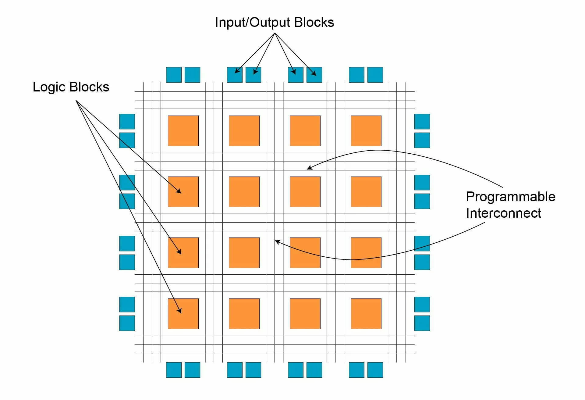
There you have it - an array of programmable gates!
To program an FPGA, rather than writing software that is compiled into machine code, flashed into program memory, and run instruction by instruction on a processor, you would instead write code to describe some behaviour, this is then synthesised into a configuration file which is programmed into the FPGA flash which is used to configure the FPGA at boot. The FPGA then "automatically" performs the function it was configured to do - often multiple functions in parallel.
Why use an FPGA?
Pros and Cons
There are a lot of trade-offs both for and against an FPGA when compared to using an ASIC (Application Specific Integrated Circuit) or MCU (Micro Controller Unit). I'll do my best to cover the generic pros and cons, but I'll be brushing over a lot of nuance.
An ASIC is the ideal solution for maximising power efficiency and speed. As it is completely custom, everything is dedicated to the end function that it will perform. The downside is that they are time consuming and expensive to develop, and so this only makes sense if you can be sure that a significant amount will be manufactured. Custom ASICs are by and large out of reach for hobbyists.
This is where MCUs and FPGAs come in. They are designed to be applicable to enough generic use-cases that they will have mass usage across a wide range of applications that designing the custom silicon for these applications make sense.
A microcontroller goes about achieving this generic applicability by using software, it reads instructions from programmable memory which conform to a predefined instruction set and then executes these functions. The processor can run these instructions as efficiently as an ASIC can as it is purpose designed for these functions. However, it will often take many instructions to achieve a relatively simple function, making it slower and less efficient than a custom ASIC solution.
An FPGA isn't able to run as fast as the processor in a microcontroller or a custom ASIC. Because it is designed to be configured to execute any function, its speed is limited by the programmable interconnects that give it its flexibility. Instead, the FPGA wields the power of parallelism. All of the FPGAs logic cells can operate at the same time as each other, more akin to a GPU than a CPU. For specific functions, digital signal processing (DSP) is a great example, despite a slower clock speed than a MCU an FPGA can achieve a much higher data throughput.
A few additional FPGA specific considerations are:
- The size of an FPGA (number of logic cells/elements/blocks, etc.) is a key consideration. This is similar to the RAM/flash size of a microcontroller, but has a far greater influence on the price of the FPGA.
- Debugging an FPGA can be quite difficult, there are no built in "print" commands, and passing/buffering arbitrary variables to the top level isn't quite as simple as making a variable global in software. Additionally, the way complex behaviour is implemented using state machines, it's a lot slower to "throw something together" or re-arrange the order of actions in an FPGA, which generally makes development slower for a given task compared to software.
- To compensate in some ways for the obtuse debug capability, simulation is a common part of FPGA design (or at least it's very good practice to). With good test coverage and well defined specifications, it is possible to obtain a high confidence that the synthesised design will consistently work as expected in contrast to conventional software where the complexity of the interaction between all programs on the same processor makes this verification arduous.
- The "infinite" configurability of an FPGA allows it to run tasks both in parallel, but also completely separately such that errors in one section cannot influence others, unlike multi-threaded software where a single thread crashing can cause the whole thing to freeze.
Why am I using one?
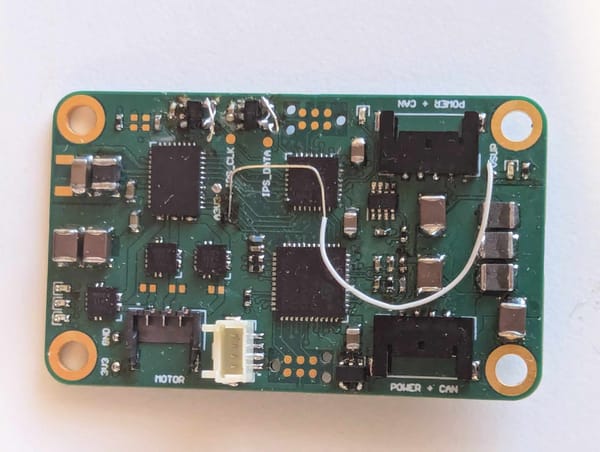
I'd be lying if I said is wasn't partly for the fun and challenge of integrating an FPGA into my motor controller. There is a more genuine reason though, specifically: more reliable real-time motor control.
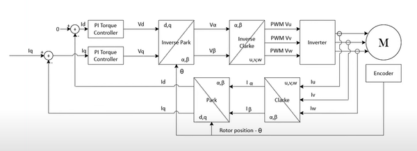
Ideally I'd like to run the full FOC motor control loop on the FPGA for completely deterministic control loop timing, but that would require interfacing with analog circuitry for the current sensing and probably floating point calculations too. This is a bit beyond what I'm prepared to tackle right now, so I've limited it to reading the position sensor and driving the PWM outputs (but maybe I'll extend this to some other bits later down the line). This also wouldn't get rid of the STM anyway (writing a CAN controller for an FPGA is waaaay beyond where I'm at right now), so it's not too bad if the STM retains some role in the motor control.
To be honest, I'm not fully sure about the conclusions in the last paragraph, but there's only one way to find out, so that's what I'm doing.
I could probably achieve this fully using the STM with proper use of the DMA & interrupts if I was better at writing embedded software, but I'm not, so I can't. Anyway, this should all help with the motor control synchronisation that I had some difficulty with last Pi-Wars, and offload some simple & repetitive processing from the STM. At least that's the theory. Maybe I'll come to regret this and delete the FPGA in Rev-B...
How do you use an FPGA?
A Few of the Basics
The parallel computing provided by FPGAs offers a different paradigm to that of conventional software. It requires a different programming language, and (for best results) a different way of thinking. I'm only going to skim over a few details here, this isn't a how to guide.
There are two main hardware definition languages (HDL), Verilog (and SystemVerilog) & VHDL. VHDL is a very verbose language, Verilog is a little more beginner friendly being fairly similar to C. System Verilog adds a few more features to Verilog, particularly on the test/verification side of things, and is my language of choice.
For best results it helps if you have a good idea of the hardware you're trying to synthesise. At the end of the day it's the compilation/synthesis tools that do this, but if you write HDL like you do software with only a high-level behaviour in mind, you won't get great results. As such, despite the development process being almost entirely "coding", a solid knowledge of digital electronic design is (I would say) critical. I will add though that, while Verilog is a very different paradigm to any conventional software, knowledge of C/C++ syntax will probably help a lot.
Writing SystemVerilog
Explaining this succinctly to any level of quality is going to be difficult, so I'm not even going to try. Maybe at some point I'll write something to this effect, but for now if you'd like to look at learning Verilog (or SystemVerilog), here are a few decent resources.
ChipVerify.com:
Textbooks
- Digital System Design with SystemVerilog by Mark Zwolinski
Simulator
- EDA playground online HDL simulator
- Icarus Verilog Windows compatible Verilog Simulator (includes GTKWave waveform viewer)
Picking an FPGA
Ideally you would be able to do this after writing the majority of your HDL, however I often find myself in the opposite position where I have to try an guess what capability I will need from the FPGA before writing anything to run on it.
In this case I went with a Lattice MachX02 FPGA, specifically the "LCMXO2-1200HC-4SG32C".
Why? Well the IDE (Diamond) is free, and generally Lattice FPGAs are smaller and cheaper than the competition from Xilinx (AMD) and Altera (Intel) which is a little more appropriate for what I want to do with it. I went for this specific one because it came in a nice package (QFN), has a reasonable pin count for what I need (32 total, 21 I/Os), and doesn't require any fancy power sequencing (or multiple supply rails). I then went for the largest version I could to give the most flexibility later down the line, which gave me a meager 1280 LUTs - not terrible, but far more restricting than the 256kB of flash the STM32G4 I'm using has.
Unfortunately it requires a fairly pricey programmer, but there's a separate post (tangentially) related to that.
Simulation
Wiggly green lines! Alright there's a lot more to simulation & verification than just staring at waveforms.
Testbenches, tasks, asserts, properties, etc. etc. There's a lot to get into here, and much like writing Verilog, I'm not going to be able to cover this here to any reasonable level of detail so I'm not going to.
Go read the ChipVerify verification tutorial pages if you're not completely boared to death by the subject already.
So What Have I Actually Been Doing?
That's all well and good, but this is meant to be a blog about progress, not a wiki. So enough of this rubbish, and back to the updates.
I've written the HDL to take in register read/write commands over SPI from the STM. One such register controls pwm output duty cycles, while another automatically updates with the motor position which is read from the hall-effect position sensor. I've simulated the key parts of this just enough that I have some confidence that I've fixed all of the major bugs, and the next step will be to program the FPGA with the latest design and run some simple motor control tests.
I still need to write the software side of the STM to FPGA interface, but if all goes well my next post will be about the first phase of motor control testing for the new motor control boards. That or a rant about FPGA development and integration. Fingers crossed.

