A Brief Tangent on Capacitors
Well, maybe not all that brief...
Ok, so I haven't made much progress on projects recently, but I'd like to post something technical and I'm hoping that maybe someone reading might find this useful, or at least interesting. If nothing else it'll make me feel slightly less bad for not posting anything for a while again.
This is a small collection of information that I've gradually picked up over the past couple of years or so about using ceramic capacitors for local and bulk decoupling. You might expect this to be a pretty limited topic, but turns out there's a whole heap to get your head around once you delve below the surface. This post will cover a handful of topics surrounding choosing a capacitor, and then about placing it along with its associated connections.
Things I Won't Be Talking About
There are a lot of topics adjacent to what I'm talking about that I won't be covering here, as well as information that is relevant in one situation and not in another, and I'd like to try to make that a little clearer upfront in the hope of mitigating future confusion.
I'll be focusing almost exclusively on surface mount technology (SMT) rather than through-hole (THT) - it's all I use now and is well within the grasp of even relatively basic hobbyists. A few bits later on regarding layout assume multi layer boards with full internal GND and power planes. Again 4+ layer PCBs are well within scope for hobbyists these days (thanks JLC!).
Ceramic capacitors will be the primary focus with regards to capacitor type. I'll briefly mention a few other types, but mostly just as an aside. Anything more exotic than these is way outside of the scope of what I'll be covering here.
MLCC
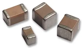
Multi-Layer Ceramic Capacitors are used on pretty much every circuit board these days, and often in staggeringly large quantities. The advent of multi-layer technology has allowed for the miniaturisation of ceramic capacitors and made their use much more prevalent. They don't come without a handful of drawbacks, however, which can be pretty significant in some cases. That doesn't mean they shouldn't be used though - in many ways they are the most "ideal" type of capacitor, it just requires the knowledge to understand and design around their main limiting factors.
Just a quick note - this section, and the following ones on layout, specifically refer to multi-layer ceramic capacitors. I imagine a majority of this would apply to single-layer ceramics, but anywhere I refer to "ceramic" capacitors assume there is a leading "multi-layer" in front of it.
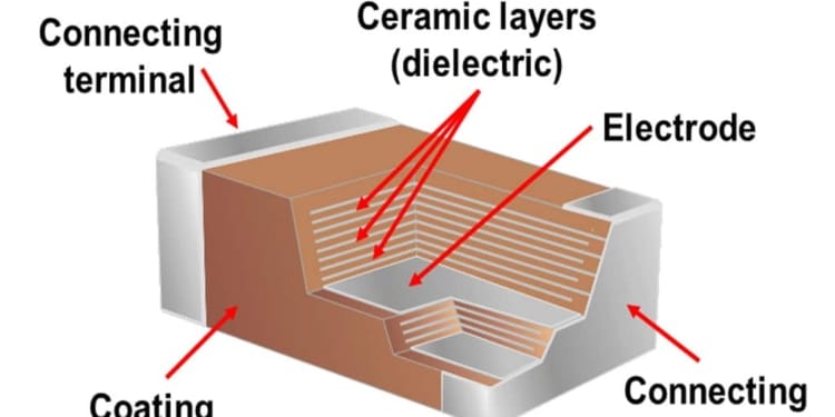
Generic MLCC Construction
Multi-Layer capacitors are constructed, as I hope you would guess, in multiple layers of capacitor plates. These layers are interleaved with alternating plates connected to each terminal of the component, effectively creating many small capacitors in parallel with each other. Multiple capacitors in parallel sum their individual values to get the total effective value, creating a high(er) density capacitor.
Capacitor Parameters
There are a handful of parameters and ratings that ceramic capacitors come with. Some are more obvious, such as capacitance, but others not so much. Some are well known, but I think they often don't get the attention they deserve, like voltage rating, and others such as dielectric and ESL are often completely ignored.
It frustrates me to no end when schematics, particularly those for reference designs, don't show the voltage rating, dielectric, & size alongside the capacitance, as this alone is not enough to understand and evaluate the suitability of a given capacitor within a design.
I'll go through some of these parameters that I think deserve a little time in the spotlight now.
Dielectric & Class
Dielectric, the bit in-between the plates of the capacitor, can be somewhat ignored in many cases. As long as the capacitor doesn't use a terrible dielectric, and isn't in an application the requires a highly stable capacitor, you can for the most part get away with it. I'd argue that you should really know what it is and the implications it can have before you go about doing that though.
Ceramic capacitors mainly come in one of two classes of dielectric materials, class 1 & class 2.
Class 1 capacitor dielectrics (typically C0G/NP0) have a vastly superior stability over their range of temperature (and lifetime). C0G/NP0 have a 0 ±30ppm/°C tolerance specification - giving less than ±0.3% variation in capacitance from -55°C to +125°C.
Class 2 capacitor dielectrics on the other hand are a little more variable, or in some cases a lot more variable. Their codes are made up of three digits, common ones are displayed from the table below:
| 1st - Letter | Low Temp (°C) | 2nd - Digit | High Temp (°C) | 3rd - Letter | Tolerance (%) |
|---|---|---|---|---|---|
| X | -55 | 2 | 45 | P | ±10 |
| Y | -30 | 4 | 65 | R | ±15 |
| Z | 10 | 5 | 85 | S | ±22 |
| 6 | 105 | T | +22 / -33 | ||
| 7 | 125 | U | +22 / -56 | ||
| V | +22 / -82 |
For example, an X7R would have a temperature range of ±15 between -55°C to +125°C. This is in the upper range of class 2 capacitors, and yet significantly worse than the class 1 performance. The upside - class 2 is a lot cheaper, denser, or some combination of the two.
As a rough rule I try to aim for X5R or X7R for most of my capacitors. If I'm struggling for choice with regards to price or capacitance/voltage vs size, then the worst I'd usually accept is Y5S. I tend to only use C0G/NP0 in specific situations that demand the extra accuracy/stability, however for some smaller values of capacitance they're cheap enough that I'll use them regardless.
A final note here - don't confuse the X or Y in the first letter of some class 2 dielectrics with class-X or class-Y capacitors - these are "safety" capacitors, often used in mains power supplies.
ESL & Size
This is another point that I think doesn't get as much attention from the average hobbyist (or engineer...) as it should. ESL, or equivalent series inductance, can in some cases be even more important than the capacitance. That might seem a little strange given that it's called a capacitor, but take a look at this example plot of impedance against frequency:
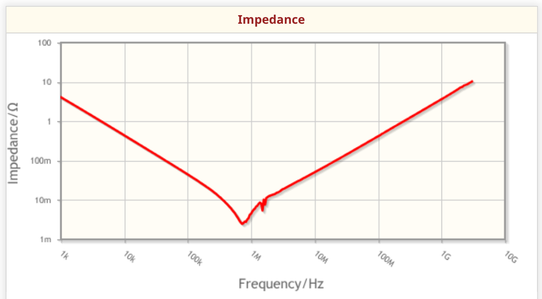
It starts as you would expect for a capacitor, high(er) impedance at low frequency which decreases as the frequency increases. But at around 1MHz the impedance starts going up?! This is caused by the parasitic internal inductance of the capacitor terminals (the ESL) which is not present in an "ideal" capacitor.
Now the parasitic inductance is a pretty minuscule value, but it's still important as it's in series with the impedance of the capacitance (the total impedance of the capacitor being the sum of these impedances). At high frequencies, where the impedance of the parasitic inductance is high and the impedance of the capacitance is low, then the inductance characteristics will dominate. So suddenly our capacitor is inductor - not ideal at all.
This is a real problem when trying to perform high frequency local decoupling. In this case, where a low impedance at high frequency is desired to "short circuit" the high frequency noise, the parasitic inductance is way actually more important when determining performance than the actual capacitance.
While you could look at every capacitor you use to find the impedance-frequency characteristics, ain't nobody got time for that. So as a rule of thumb, the smaller a capacitor is the lower the ESL tends to be. This is due to the terminals (and capacitor height - more on this later) which contribute to the ESL being smaller. You should be aiming to place the smallest sized capacitor you're willing to use as close as you can to each IC power pin you're decoupling (going too small will increase assembly cost and difficulty, I usually go for 0402 as a reasonable balance for this).
For bulk capacitance decoupling/filtering this is less of an important factor as the frequencies these are aiming to filter are much lower. This works out fairly nicely since the currents are also likely to be larger (lower frequency so exist for longer durations), which necessitate a larger capacitance in order to filter (in a larger package) which will tend to come with a higher ESL anyway.
Voltage Rating
This one's a bit of a gotcha - it feels straightforward, but has more intricacy than it lets on. You might naively assume that, like the power rating on a resistor or maximum voltage on an IC, if you stay just below the rated value (or maybe a little under to leave some margin) that it'll work fine. However that's not the case.
Ceramic capacitors tend to have significant de-ratings applied to them with DC biases applied to them, even far below their rated voltage.
When using capacitors for filtering a DC supply, particularly at the input and output of a power supply (but also for local decoupling to some degree), check the datasheet/manufacturer's website to see what the actual capacitance value is likely to be.
The example below works through the numbers for a specific part, just to give an idea of just how bad this can be in many cases.
DC Bias de-rating
MPN: C2012X5R1A476M125AC is a good example of a capacitor that you might use for bulk capacitance at the output of something like a 5V power supply.
It has the following datasheet specifications:
- 47uF capacitance
- 10V voltage rating
- 0805 package size
- X5R dielectric/temperature rating
Say we have a 100uF target output capacitance, 2 of these should get us pretty much all the way there, and there is plenty of headroom on the voltage rating (100% margin), so what could possibly go wrong?
Looking at the manufacturer website for a little more information we see this graph:
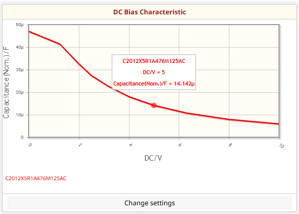
And therein lies the problem, you only get the specified capacitance with pretty much 0V of DC-bias across the capacitor, not exactly a realistic scenario for a decoupling capacitor on a power supply rail.
At our 5V nominal voltage rail, instead of around 100uF of capacitance with 2 of these we instead have around 30uF, less than a third of what we were expecting. Even on a 3.3V rail we're looking at about 50% loss of capacitance for ~50uF total instead of 100uF.
Caveats
It is important to note, this doesn't rule out using this capacitor for this purpose - 15 or 25uF in an 0805 package is still pretty good, and finding a capacitor with a higher voltage and therefore less de-rating is likely to end up resulting in an even larger package size (with more ESL). Putting several of these in parallel (further decreasing the ESL between them) is a good (perhaps even great) way of getting a large amount of bulk capacitance, you just need to be aware of it in the first place so that you know that more capacitors will be required than their value might initially suggest.
It's also worth noting that this is much more an issue for bulk decoupling where the extra capacitance is actually required. For local decoupling, this effect can largely be ignored on local decoupling capacitors (as long as there is at least some reasonable margin), as the high frequency currents that we're aiming to smooth out near the device will generally not come close to actually depleting the capacitor. As in the above section, the impedance characteristics of the capacitor with respect to frequency are more important than the overall value of the capacitor itself when performing local high-frequency decoupling.
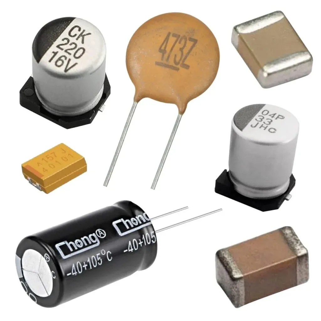
Other Types of Capacitor
I'd be remiss if I didn't mention a couple more types a capacitor technology before I move on to some of the practicalities & layout considerations of using ceramic capacitors.
Electrolytic
I'm sure most people know a reasonable bit about these already (and there's a lot less nuance going on here). The most common type are aluminium electrolytics. As compared to ceramic capacitors they:
- Come in much larger values of capacitance (for the size & cost) - good for bulk decoupling
- Are polarised - good for DC supply decoupling, no so much for AC (pretty good fun to wire up in reverse and watch them pop though)
- Have fairly high ESL & ESR - bad high frequency characteristics, fairly useless above a few hundred kHz
- Lose capacitance as they age (to the point that they can eventually completely fail)
- Don't de-rate with DC bias in the same way as ceramic capacitors
There are also aluminium polymer electrolytic capacitors, these improve the ESR characteristics as well as improving the aging/lifetime issues by using a solid electrolyte. In return they tend to be more expensive - nothing's ever free.
Tantalum
Strictly speaking these are also electrolytic (use an electrolyte), but people tend to mean aluminium when they say electrolytic. Or at the very least I do.
Tantalum are relatively niche in hobby electronics, likely due to their price. Other than cost, they are fairly similar to aluminium electrolytics - polarised, high volumetric efficiency, and high ESR. So why would you use them? Well they don't have the same aging issues as aluminium (or aluminium polymer) capacitors.
Decoupling Capacitor Objectives
From Chapter 11 of Henry Ott's "Electromagnetic Compatibility Engineering", a summary of the goals when performing power supply decoupling:
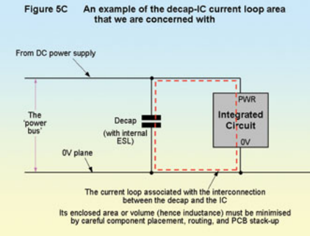
This gives a pretty good overview of the target - minimise parasitic inductance by providing a current path with the smallest loop area/volume possible (including vertically).
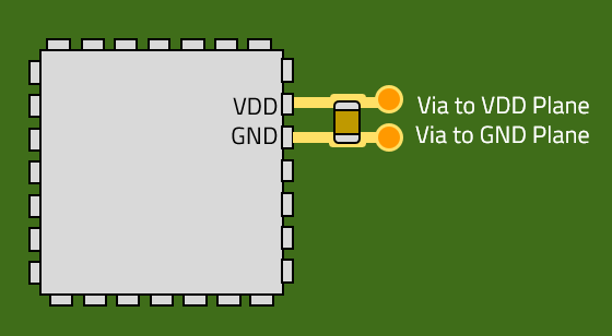
At all costs (for high frequency decoupling - which is the case for almost everything digital due to the rate of the switching edges), the inductance between the active device and the decoupling capacitor (depicted in Figure 5C below) as well as the device to the power planes should be minimised. This is achieved by minimising the loop area/volume of the current path.
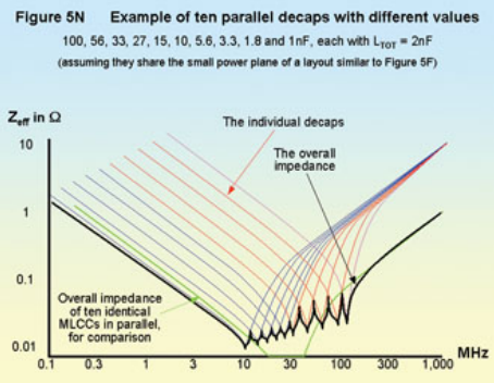
Size & Number of Decoupling Capacitors
The myth of the three capacitor values is an article "debunking" legacy best practice guidelines for power supply decoupling based on through-hole component characteristics, and well worth a read.
The diagram below provides an example of the resonant peaks that can be caused by "decade decoupling", compared to the dotted line of several identically sized capacitor with the same size as the largest decade capacitor.
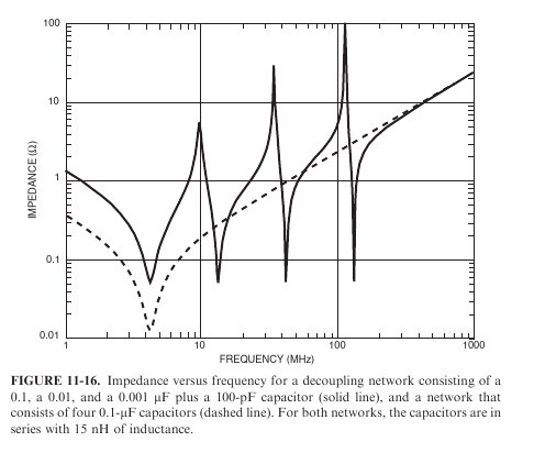
This isn't to say that multiple values of capacitors should never be used (see Figure 5N below for an example of a well designed solution to create a greater low impedance frequency range). However, if you aren't simulating a realistic parasitic inductance when designing your PDN (Power Distribution Network) filter it's probably best to try and stick to all the same value.
You also shouldn't take for granted manufacturer datasheets that recommend things like decade capacitances - these are likely grandfathered from old designs which were intended for use with leaded components.
The "100nF rule" is usually pretty good as a rule of thumb - one 100nF capacitor for every power pin of an IC. This is chosen as a reasonable balance between having enough capacitance (including after DC-bias de-rating) that it will have enough capacitance to meaningfully smooth out power supply ripple, while being a low enough value that it can be found in a small package with reasonably low ESL, and therefore good high frequency decoupling performance. If the IC is particularly big, power hungry, or the manufacturer recommends it, I might also put a 4.7uF or 10uF capacitor nearby to the chip as a "local-bulk" decoupling capacitor.
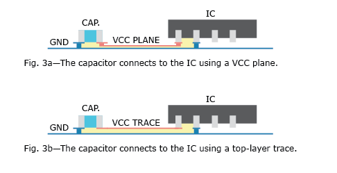
Connecting Capacitors & ICs
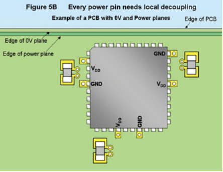
The impedance of the scheme shown in Fig. 3b below is lower than that of Fig. 3a, despite having a higher resistance due to 2 extra vias on the Vcc connection, this is negligible at high frequency (where decoupling capacitors are most important) compared to the decrease in inductance caused by the lower loop area of the current path. An alternate view of this is shown in Figure 5B below. These (and much of this Section later on as well) assumes that the stack-up has a power and ground plane that are closely coupled. If not, then some of these rules of thumb will not be ass applicable.
Note that also connecting Vcc on the top layer is acceptable as this would re-introduce the higher inductance connection but two inductors in parallel result in a lower inductance than any one inductor. The majority of the high frequency component of current flow will still follow the lower inductance route through the vias though (much like how high frequency signal return currents on a microstrip trace will flow directly below the trace). When doing this you should be very careful to ensure that all pins have a via nearby though - the top layer connection should be an extra on top of the vias. DRC will not throw an error for things like this (unless you put a lot more effort than I do into your PCB design rules), so it takes care & attention.
From SigCon - Bypass Capacitor Sequencing (left) & Advanced PCB design and layout for EMC - Part 5 Decoupling, including buried capacitance technology (right)
So this reveals something pretty important to good decoupling capacitor performance which, for a long time, I'd never really thought about - designing the stackup to ensure that the power and (one of the) GND planes are located as close to each other as possible can make a huge difference.
They should be adjacent to each other, and ideally be located as close together as the stackup allows. For example on most 4-layer stackups the 2 inner layers, while adjacent, are located relatively far away from each other and should therefore not be used for a power and GND plane pair.
As well as reducing the parasitic inductance of the power supply decoupling loop, placing these planes next to each other can even create a board-wide capacitor of sorts. This has negligible effect when the planes are too far apart, but once they are very close it can actually provide significant intrinsic decoupling across the whole board.
Decoupling Capacitor Via Placement
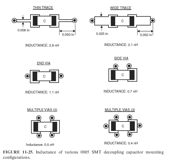
Delving further into via placement for minimising inductance, we can see that we should use short & stubby traces. This is easy enough to understand from a resistance perspective, but is crucial for minimising inductance as well.
Placing the vias on the side of the capacitor reduces the inductance compared placing them at the ends (with generally minimal impact to board space), It is easy to understand when looking at the capacitor from the side, rather than from above, that this decreased the loop area created by the vias between the capacitor and power/ground planes. Note that this is only because capacitors tend to be longer than they are wide, if you have a capacitor that had an inverted aspect ratio then it would make more sense to place the vias at the ends.
Maximising the number of vias also reduces inductance as before by making parallel paths for the current to flow (although space constraints will often make this more difficult to perform).
Note that taller (read larger) MLCC capacitors increase the loop area since some of the current must travel further up the case of the capacitor to reach the upper layers as shown in the figure below. This is why physically larger capacitors tend to have larger values of ESL (equivalent series inductance), and therefore why the smallest possible capacitor (balancing manufacturability) should be used to achieve the best local high-frequency decoupling.
For this reason, vertically stacked capacitors should be avoided, certainly for local decoupling, but also in general where possible. They save board space, but will have significantly more inductance compared to what the same capacitors would have if mounted side by side on the same board.
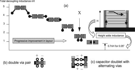
PCB layout for high frequencies:
Assuming you will be using small chip multilayer ceramics, with a package size of 0402, 0603 or at a pinch 0805, the determining factor for the inductance of the component is its PCB layout. This is illustrated in Figure 13.13(a). The two pads of the capacitor are taken through vias to the relevant power and ground planes; the length of the pad-to-via track, separation of the vias, the dimensions of the capacitor and the height of each via between the surface pad and the buried plane determine the overall loop area, and hence the inductance contributed by the layout. If the board costs are to stay low then the vias should not be placed in the pads, so layout ‘X’ is the best option. If you double the vias (b), a plus and minus pair close to each other on each side of the component pads, this nearly halves the overall inductance and is largely cost-free. Archambeault [24] has pointed out that an even better approach is to create a doublet of a pair of capacitors with alternating opposing vias (c): here the proximity of the plus and minus pair of vias is used to best effect.
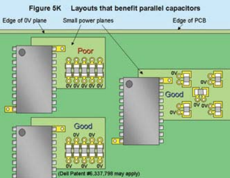
When adding multiple parallel capacitors (ideally of the same value as per the section on size & number of decoupling capacitors), the image below shows some rule of thumb guidelines (Figure 5K).
Vias should placed to the side with capacitors spaced out evenly, or if laid out in a row, the capacitors should be placed in alternating polarities so that the end vias alternate (similar to the capacitor doublet shown in the image above). It is tempting to lay them out in a row next to each other as this minimises board space due to the clearances required between different nets but this should be avoided for local decoupling. For bulk decoupling using larger capacitors (in both value and physical size) this is less of an issue, for one because the parasitic inductance is less of a concern, but also because there is likely room to fit vias in-between the pads of each capacitor rather than needing to use the sides or ends.
Further Examples of Good & Bad Decoupling Capacitor Placement
Initially, the example below would appear to be good, as there is a relatively short loop between the Vdd pins and the capacitor, however the only vias to the power/ground planes are far away from the device pins meaning that there is far more inductance there than is required. Additionally, while the return loop for the Vdd trace is short, the return path for any signals to/from the chip will have a much longer loop.
Since clearance constraints almost always mean that there will be space between the device and the decoupling capacitor, vias should be placed in-between the capacitor and the device. Even if there is not already space, it is better to push the capacitor further away from the pins it is meant to be decoupling in order to ensure the vias are close to the power pins. As the GND pin forms the return loops for more pins than just Vdd it is more important for this to have a close via, but ideally both the GND and Vdd pins would have close vias.
If there is only space for one set of vias, it is far better to place them in between the capacitor and the device, but keeping the set on the far side as well is desirable.
The capacitor placement shown in the picture below is almost never appropriate. If a printed circuit board has a GND plane, the GND pins of the active devices should generally connect directly to the plane with no intervening trace. High-speed active devices should not share their GND plane connections with any other component, including decoupling capacitors. The GND pin of an active device is usually part of the return-current path for single-ended signals. It should have a low-inductance connection to the current return plane (on this board labelled GND plane). Attempts to force the current in this connection to pass under a decoupling capacitor increase the connection inductance and do nothing to improve the power bus decoupling
In the example below, b is the best option as it provides the smallest loop area for the current flowing between the active device and the decoupling capacitor despite the others being in closer proximity.
This is enabled by a closely coupled ground and Vcc plane which provide an incredibly low inductance path between the vias.
In this example it doesn't matter much which side the decoupling capacitor is placed as the power and ground plane pair is located roughly centrally in the board stackup. However, if they were placed closer to the top side of the board for example, then it would be desirable to have all of the active devices and decoupling capacitors on the top side to minimise the vertical loop area introduced by the vias from the device and capacitors to the power & ground planes.
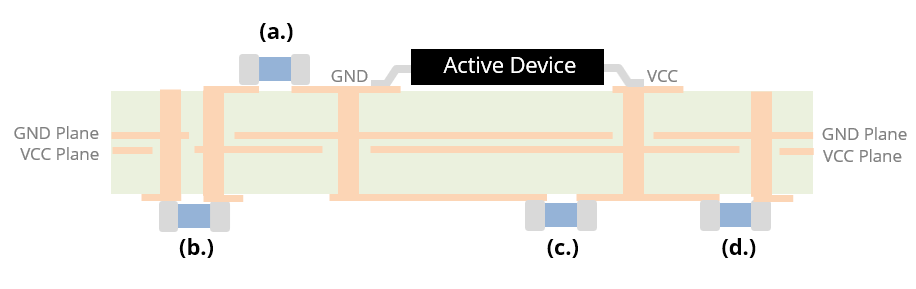
With an active device mounted on an 8-layer board with a GND plane on layer 4 and a VCC plane on layer 5, b) provides the best high-frequency decoupling. When power is distributed on closely-spaced planes beneath the active component, the decoupling capacitors with the lowest-inductance connection to the planes are best able to provide charge to the active device quickly. Option (b.) minimizes the connection inductance by connecting directly to the planes through vias that are near each other. Options (a.), (c.) and (d.) all have traces between a capacitor pad and at least one of the via connections. In fact, option (c.) [which was recommended in a recently published application note] is by far the worst option. On boards with a solid GND plane, the GND pad of a decoupling capacitor should always connect directly to the plane.
For BGAs it is common practice to place decoupling capacitors on the opposite side of the device below the power pins, however we have seen above that the proximity of the capacitor isn't the most important factor. However, this is often still a good practice due to the difficulty/complexity of breaking out large pin count BGA devices. As there will already be through-vias from these power pins to connect them to the power & ground planes, then on the opposite side of the board there are already low inductance connections which can accommodate a decoupling capacitor. Additionally, if the power/ground planes are located centrally in the stackup then it is perfectly acceptable to locate the decoupling capacitor on the opposite side to the BGA device (or even preferred if the BGA must be placed on the side that is more distant to the power/ground planes).